If the PCB is sealed with solid sealant, how to determine the creepage distance and clearance?
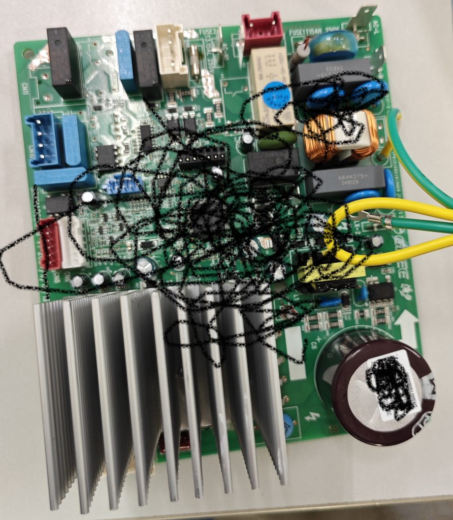
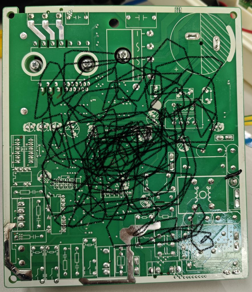
functional insulation as well as other insulation exists on circuit boards. Typically, the surface environment of a circuit board is determined to be either Pollution degree 3 or pollution degree 2.
If the circuit board is mounted in an electrical box and sealed with a solid sealant, the sealing will look as follows:
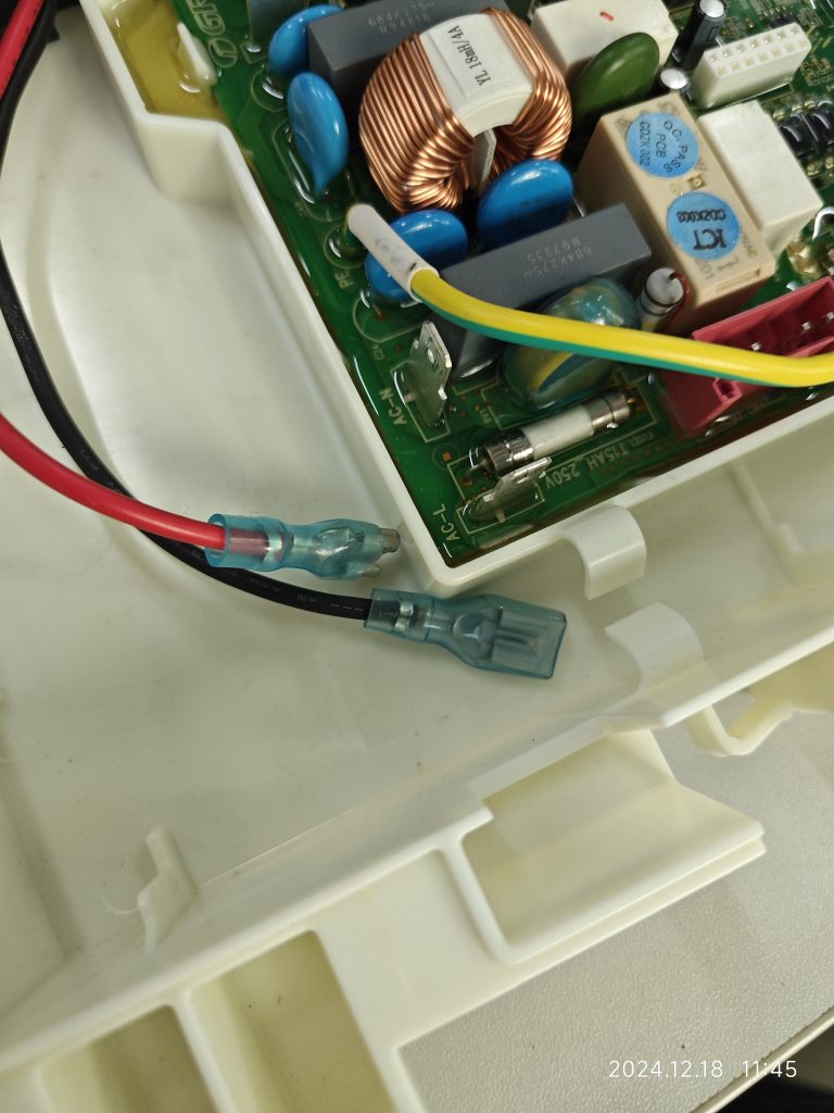
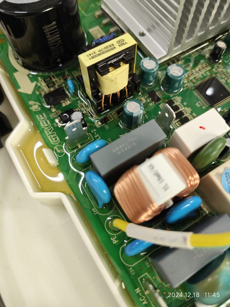
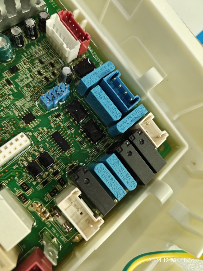
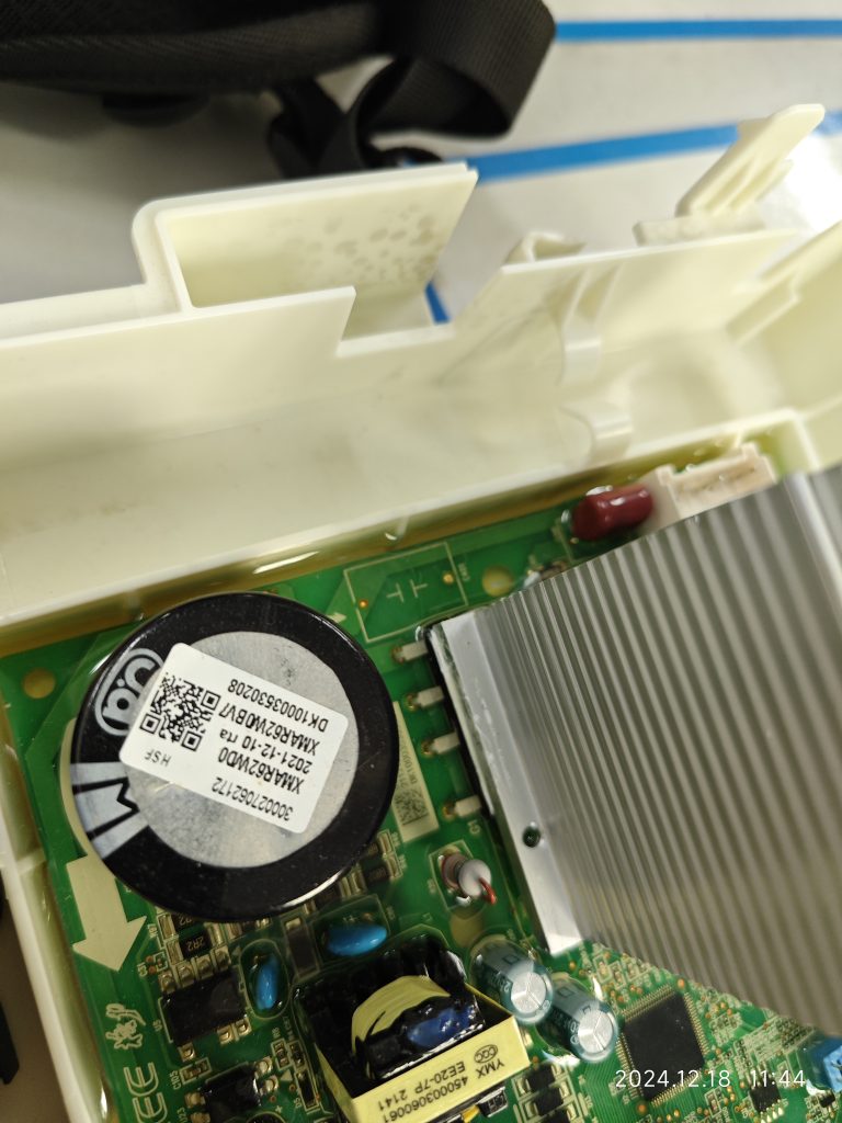
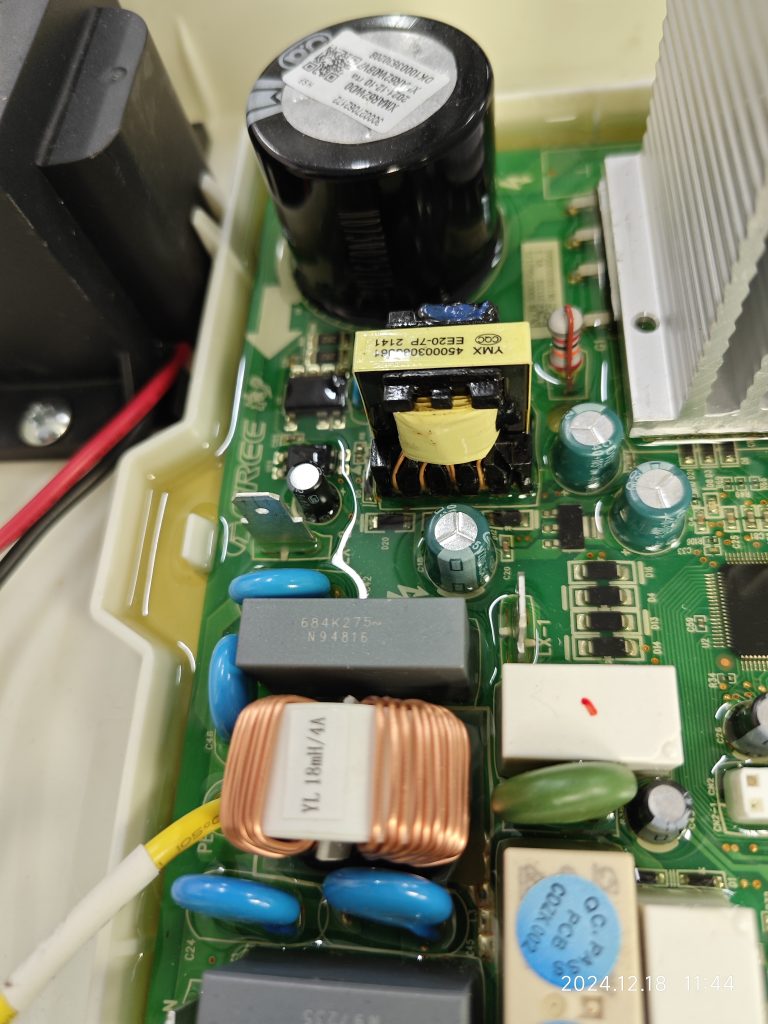
What should be the pollution degree of the functional insulation between the copper tracks on the PCB and between the energized parts on the component?
Here, the functional insulation is located inside the solid sealant and there is no contact between the path of the functional insulation and the outside air. According to the definition of electrical clearance, it can be assumed that there is no electrical clearance here. At the same time, the creepage distance is defined along the surface of the insulation, and obviously, there is no surface here either.
It may be argued that there is still a gap between the solid sealant and the PCB material, and that an clearance and creepage distance can be formed, but it is a pollution degree 1. This view is more conservative, because even if a gap is formed, it is not a continuous gap.
At the same time, the pictures show that this solid state sealant fills so well that it is essentially impossible to create a gap. The manufacturer also indicates that there is a vacuuming procedure prior to filling the solid state sealant. When we evaluate this type of structure, we can have some control over the material and specification of the solid state sealant, as well as some control over the filling process.
There may also be reinforced insulation internally, as there are isolation measures between the 220-240V circuit portion and the SELV circuit, which are judged by the same rules for clearance and creepage distances as functional insulation.