How are the creepage distances and electrical clearances of PTC heating element surfaces determined?

We are discussing here the second structure of the PTC heating element, PTC heating element structure please refer to the explanation of its definition.

figure 1
figure 2

How is the creepage distance of the functional insulation at the location of the red circle in Figure 1 determined?
We all know that NOTE 1 of TABLE 18 section has the following requirements.
NOTE 1 For PTC heating elements, the creepage distances over the surface of the PTC material need not be greater than the associated clearance for working voltages less than 250 V and for pollution degrees 1 and 2. However, the creepage distances between terminations are those specified in the table.
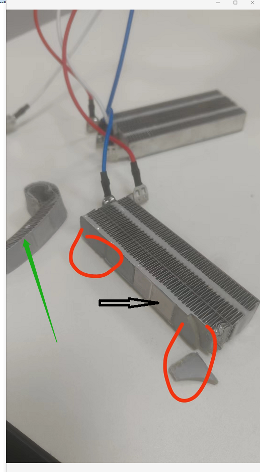
In the first case, the heating units are fixed by means of a conductive adhesive and a heat sink, with some gaps between the heating units, but all the gaps are filled with an insulating adhesive.
As shown in Fig. 2, the heatsinks connected to the fire wire and the heatsinks connected to the zero wire are functionally insulated by means of an insulating structure filled with adhesive, whereby the electrical gaps and creepage distances are formed by the upper surface of the insulating adhesive. Since the environment in which the PTC heating elements are located is of pollution class III, then NOTE 1 of the TABLE 18 section does not apply. Therefore, the requirement for creepage distance is 3.2 mm if it is determined according to the 250 V operating voltage, but of course, we need to use the interpolation method to calculate the creepage distance limit at the rated voltage. Usually, the gap between the two heat sinks is about 2.4mm, then its resulting creepage distance and electrical clearance is generally 2.4mm, the smarter approach is to raise the gap on the insulating adhesive, made into a curved projection, which lengthens the creepage distance and electrical clearance.

The second case, the heating unit through the conductive glue and heat sinks are fixed, leaving a certain gap between the heating unit, but the surface of the heating unit are attached to the insulating adhesive.
And the requirements of the first case is the same, just the middle of the gap if you increase the creepage distance of the problem. In fact, it is not difficult to think of, can be in the middle of the gap near the location of the heating unit to increase the glue, glue can not be laid flat on the side of the heating unit, need to be laid into a U-shaped. Of course, this process is more difficult to realize, not recommended.

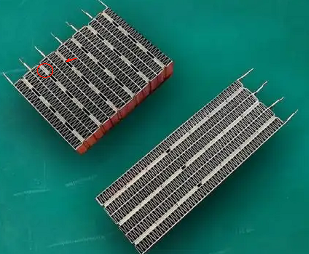
In the third case, the heating unit is only fixed by the conductive glue and the heat sink for sticking, and there is a gap between multiple heating units. See Figure 1, the upper left corner of the component. There is no insulating glue attached between the heat generating units or on the surface.
The electrical gap is present in the gaps. What is in dispute here is how to determine the creepage distance. According to conventional logic, there is no creepage distance. According to the definition of creepage distance, creepage distance is in the surface of the insulating material trip, two heat sinks between the heating unit is not an insulating material, so its surface can not form a creepage distance path. Since no creepage distance can be formed, the prerequisite of clause 29.2.4 is not satisfied, and therefore there is no need to assess the creepage distance of functional insulation.

However, I personally still believe that we need to consider creepage distances, because the existence of creepage distances also takes into account the deposition of contaminants on the surface of a material, which can lead to short circuits. Here the PTC heating element generally work in Pollution degree 3, the surface must be for the accumulation of a lot of pollutants, pollutants, if too much, will lead to functional insulation short-circuit, resulting in appliances or power supply lines in the protective device action. This is in fact a less safe means, and the standard does not allow for the operation of protective devices in the supply line.

Similar Posts

  • |

    If the PCB is sealed with solid sealant, how to determine the creepage distance and clearance?

    functional insulation as well as other insulation exists on circuit boards. Typically, the surface environment of a circuit board is determined to be either Pollution degree 3 or pollution degree 2.If the circuit board is mounted in an electrical box and sealed with a solid sealant, the sealing will look as follows: What should be…

  • 第 3 項 – 「保護インピーダンス」の定義の理解方法

    保護インピーダンス: 通常の使用時および機器の故障の可能性がある状態での電流が安全な値に制限されるように、クラス II 構造の充電部分とアクセス可能な導電部分の間に接続されたインピーダンス。 ケース1:最初のケースは、通常、アダプター駆動の製品など、低電圧電源を必要とする状況です。アダプターの出力電圧はDC12V、DC24V、またはDC5Vです。これらの低電圧部品は、変圧器の変圧と整流器電流の整流によって得られるため、一般にユーザーが触れることができます。したがって、高電圧部分と電圧部分を効果的に絶縁する必要があります。当社の一般的なスイッチング電源基板では、EMC 伝導テストを実施すると、トランスの一次側で発生した干渉が一次側と二次側の間の寄生容量を通過し、150k~30MHz の伝導性干渉が発生して二次側に到達します。ここでは、Y コンデンサを使用して干渉信号を電源に戻し、干渉を相殺するループを形成します。そうしないと、導通テストが不合格になります。ここでの Y コンデンサは保護インピーダンスを形成します。下図の赤いボックスで選択された 2 つの Y コンデンサが保護インピーダンスです。 下図はマイナスイオン発生器の回路図です。赤い四角形で選択された 2 つの抵抗は、一般的な保護インピーダンスです。 下の図のCY1とCY2は保護インピーダンスですか? 規格の定義から、保護インピーダンスは接地が存在するクラス II 構造で使用されます。ここでの接地が保護接地として定義されている場合、保護インピーダンスはクラス II 構造で使用され、ここではクラス I 構造であるため、明らかに CY1 と CY2 を保護インピーダンスとして定義できません。ここでの接地が機能接地として定義されている場合、2 つの問題があります。まず、これはクラス I 構造であるため、CY1 と CY2 は保護インピーダンスとして定義できません。次に、クラス II 構造の場合、CY1 と CY2 を保護インピーダンスとして定義でき、保護インピーダンスの関連要件を満たす必要があります。私の個人的な意見は、CY1 と CY2 は保護インピーダンスではなく、直接基礎絶縁とみなしてよいと考えています。結局のところ、回路図に示されている設計は規格に受け入れられないということでしょうか?そしてnbsp; それらが保護インピーダンスである場合、どちらが第 22.42 条「保護インピーダンスは少なくとも 2 つの別個のコンポーネントで構成されなければならない」に準拠する必要があります。 From the definition of the standard, the…

  • Clause 3 – How to understand the definition of “accessible part”

    accessible part: part or surface that can be touched by means of test probe B of IEC 61032, and if the part or surface is metal, any conductive part connected to it.NOTE Accessible non-metallic parts with conductive coatings are considered to be accessible metal parts. There are some parts or surfaces in the appliance that…

  • 第3項「定格入力」の定義の見方

    定格入力電力:メーカーによってアプライアンスに割り当てられた電源入力記入への注記 1: 機器に電源入力が割り当てられていない場合、加熱機器および複合機器の定格入力電力は、機器が定格電圧で供給され、通常の動作で動作したときに測定された電源入力です。 一般に、メーカーは、最大電力入力の条件下で定格電圧で動作する製品によって生成される入力電力に基づいて定格電力入力を決定する場合があります。これは、10 項の電源入力テストでは、製品が定格電圧で動作する必要があるためです。一部の製品には特殊なケースがある場合があり、これについては後続の章で説明します。 経験豊富な開発チームの場合、製品設計の初期段階で定格入力が決定され、開発者は設計プログラムに従って製品を設計します。また、開発者が設計スキームを持っておらず、製品試作後に定格入力を暫定的に確認するケースもあります。ルームヒーター(石英管ヒーター)などの製品の定格電圧はAC220Vですが、通常はAC220V電源で製品を使用することができ、ヒーターの動作状態は最高レベルの熱に設定されます(首振りやその他の機能がある場合)をオンにする必要もあります)。これは、実際の入力電力、丸め値を定格電力入力として記録します。したがって、第 10 項の電源入力試験を実行する場合、試験値と定格値が規格で指定された偏差範囲を超えた場合、第 10 項の要件を満たすように定格入力電力を変更することができます。 ほとんどの場合、アプライアンスには定格電力入力が与えられます。製品には定格入力電流のみが与えられる場合もありますが、実際のテストでは、規格により製品の動作状態を定格入力電力に基づいて判断することが求められています。このメモの情報に従って入力電力情報を決定することができます。これはまれな状況です。製品のテスト条件が定格入力電力に基づく場合、通常、製品には定格入力電力のラベルが付けられます。製品のメーカーが入力電力定格を指定していない場合でも、サードパーティの試験機関は通常、製品をテストするときに入力電力定格情報を要求します。これは、定格電圧 AC220V、定格電流入力 10A と表示され、定格電力入力のない石英管ルーム ヒーターの仮想的な例です。第 11 項の耐熱試験を実施する場合、規格では定格入力電力の 1.15 倍で製品を動作させることが求められています。この状況では、この記事の注記の情報を使用して定格電力入力を決定できます。暖房器具には通常、定格入力が表示されています。

  • Clause 3 – How to Understand the Definition of “off position”

    off position: stable position of a switching device in which the circuit controlled by the switch is disconnected from its supply or, for electronic disconnection, the circuit is de-energized.NOTE The off position does not imply an all-pole disconnection. With reference to the content in the NOTE, both all-pole disconnection and single-pole disconnection are a stable…

  • 第3項 「第3種建築物」の定義の見方

    クラスⅢ構造:感電に対する保護が安全特別低電圧に依存しており、安全特別低電圧以上の電圧が発生しない機器の一部注記 SELV での供給に加えて、基礎絶縁が必要な場合があります。 8.1.4を参照してください。注 2 機器の主要部分が SELV で動作し、取り外し可能な電源ユニットと一緒に納入される場合、機器のこの主要部分はクラス I 機器またはクラス II 機器のクラス III 構造とみなされます。 アプライアンスはプラグイン可能なアダプター (保護接地なし) によって電力を供給され、アダプターとアプライアンスは一緒にユーザーに配送されます。アダプターとアプライアンスは合わせてクラス II アプライアンスとして判断されます。アダプターはクラス II であるため、これによって感電に対する保護のクラスが決まります。ただし、機器 – ファンのみはクラス III 構造、つまりクラス II 機器内のクラス III 構造です。 もちろん、スイッチ電源 PCB が機器に組み込まれており、このスイッチ電源 PCB が SELV 回路を提供できるという別の状況もあります。そして、SELV回路部分はクラスII構造となっております。 Of course, there is another situation, that is, a switch power supply PCB is embedded in the appliance, and…